CBED quickstart#
This notebook demonstrates a basic CBED simulation of silicon in the \((111)\) zone axis.
Configuration#
We start by (optionally) setting our configuration. See documentation for details.
abtem.config.set(
    {
        "device": "cpu",
        "fft": "numpy",
        "diagnostics.task_progress": False,
        "diagnostics.progress_bar": False,
    }
);
Atomic model#
We create the atomic model. See our walkthough or our tutorial on atomic models.
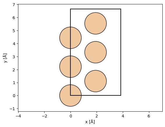
We create an atomic model of silicon using the bulk function from ASE.
silicon = bulk("Si", crystalstructure="diamond")

abtem.show_atoms(silicon, plane="xy");
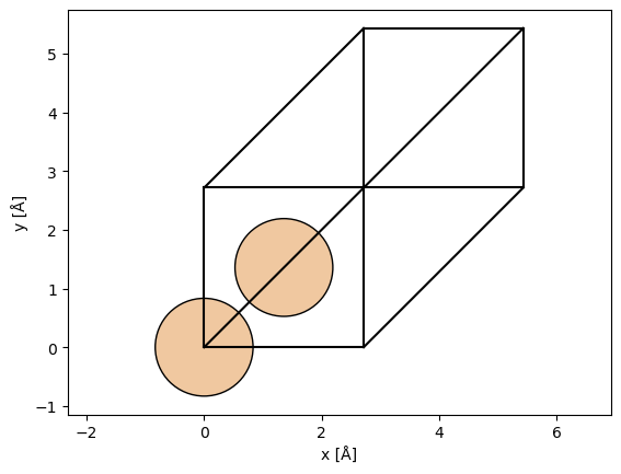
We can choose the \((111)\) zone axis to be a propagation direction using the surface function.
silicon_111 = ase.build.surface(
    silicon, (1, 1, 1), layers=3, periodic=True
)  # create surface structure in the (111) direction

silicon_111_orthogonal = abtem.orthogonalize_cell(silicon_111)  # make cell orthogonal

abtem.show_atoms(silicon_111_orthogonal);
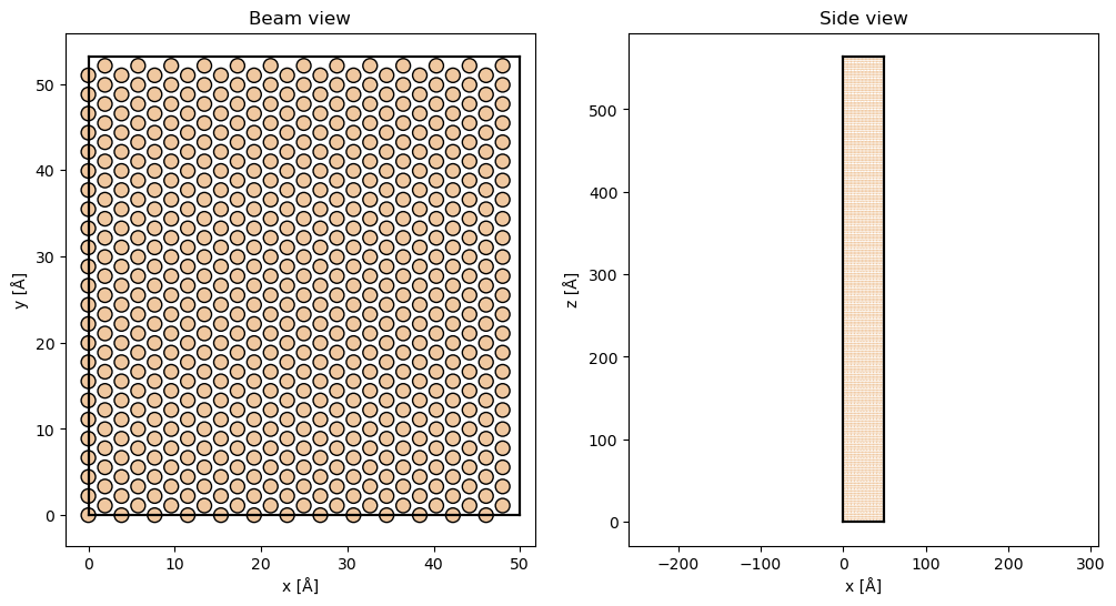
Finally we repeat the structure in \(x\) and \(y\), this will improve the reciprocal space resolution. We also repeat the structure in \(z\), thus simulating a thicker sample.
atoms = silicon_111_orthogonal * (13, 8, 60)

fig, (ax1, ax2) = plt.subplots(1, 2, figsize=(12, 6))
abtem.show_atoms(atoms, ax=ax1, title="Beam view")
abtem.show_atoms(atoms, ax=ax2, plane="xz", title="Side view", linewidth=0.0);
Potential#
We create an ensemble of potentials using the frozen phonon. See our walkthrough on frozen phonons.
frozen_phonons = abtem.FrozenPhonons(atoms, 8, {"Si": 0.078})
We create a potential from the frozen phonons model, see walkthrough on potentials.
potential = abtem.Potential(
    frozen_phonons,
    sampling=0.1,
    projection="infinite",
    slice_thickness=2,
    exit_planes=60,
)
wave = abtem.Probe(energy=100e3, semiangle_cutoff=9.4)
wave.grid.match(potential)
wave.profiles().show();
Multislice#
We run the multislice algorithm and calculate the diffraction patterns, see our walkthrough on multislice.
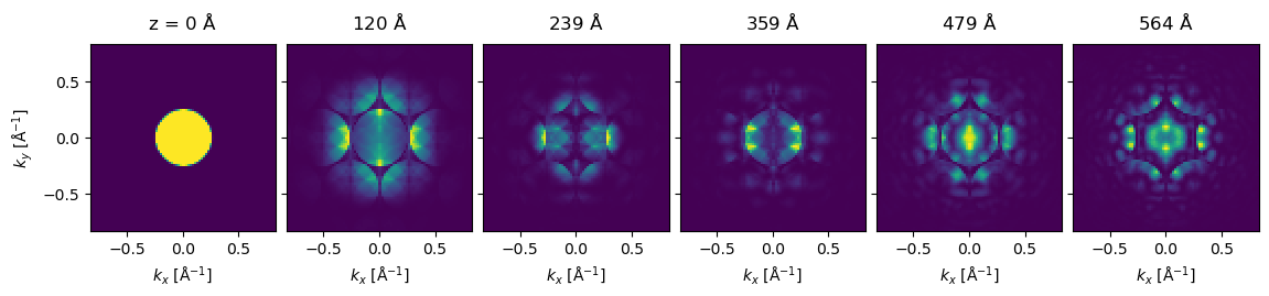
measurements = wave.multislice(potential).diffraction_patterns(max_angle=30)
We take the mean across the frozen phonons axis, and compute the result.
measurement = measurements.mean(0)

measurement.compute();
Visualize results#
We show the thickness series as an exploded plot.
visualization = measurement.show(
    explode=True,
    figsize=(12, 5),
)